Power Circuit Layout
Many circuit boards employ switching power circuits to convert a supplied power voltage to one or more different voltages required by the active components on the board. The high-frequency switching in these circuits creates noise that may show up in conducted or radiated emissions tests. The goal of the board designer is to contain this switching noise and not allow it to couple to traces or components that might ultimately carry this noise off the board.
Figure 1 illustrates how different power converters might be connected to produce the different voltages required for circuits on the board. There are many power-converter design options that employ different circuit topologies, different switching components, and different switching frequencies and modulations. The proper layout for reducing conducted and radiated emissions largely depends on the inverter topology. However, the layout is also influenced by requirements related to other factors such as heat dissipation, current-carrying capacity, proximity to other circuits, and galvanic isolation requirements.

Figure 1: Six voltages derived from one 12-volt supply.
Since the layout depends on the converter topology (i.e., the fundamental components and how they are connected), it’s important to recognize which topology a converter employs before the components are placed. There are many different converter topologies, and each has its own layout priorities for meeting conducted and radiated emission requirements. In this section, we will start by looking at the four basic topologies (buck, boost, H-bridge, and flyback) shown in Figure 2. Once we understand how to lay out these common converters, we will have the basic tools we need to make good layout decisions for virtually any other switching converter topology.
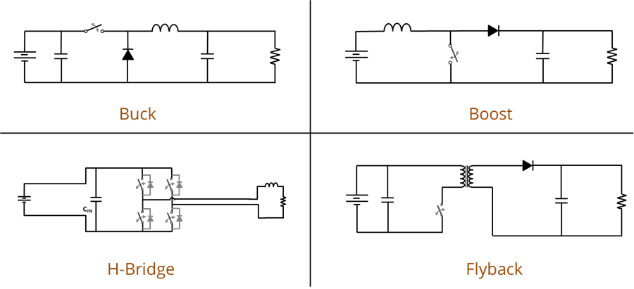
Figure 2: Four common power circuit topologies.
Developing a good grounding strategy is a fairly straightforward process. So, one might wonder why so many systems are improperly grounded. The answer is simple: engineers often confuse the concept of ground with another important concept, current return. The fact that current return conductors in digital electronics are often labeled ground or GND can be confusing. When current return conductors are treated like grounding conductors (or when grounding conductors are used to return currents), the result is often a design with significant EMC problems.
Buck Converters
Buck converters are relatively simple and employ low-cost components. They are widely used in circuit boards to convert a DC voltage down to a lower one efficiently. They can also be used in situations where a constant-current source is required. The basic topology is illustrated in Figure 3.

Figure 3: DC-to-DC buck converter topology.
The cycle starts when the switch closes, allowing current to flow from the voltage source to the load. The voltage across the load rises until the desired voltage (or current) is attained and the switch opens. With the switch open, the inductor keeps the current flowing through the load and returning to the inductor through the diode. However, as the energy stored in the inductor is depleted, the voltage across the load falls. Before it falls too far, the switch closes again, and the cycle is repeated.
An important component that is not shown in Figure 3 is a microcontroller that monitors the voltage across the load and operates the switch. Typically, the switch turns on at a set time interval, and the turn-off time is varied to control the amount of power delivered to the load. So, the switching voltage and current are pulse-width-modulated (PWM) signals with a specific fundamental frequency. Today’s low to medium-power DC-to-DC converters typically switch at frequencies between 1 and 3 MHz, with PWM modulations designed to range from about 10% to 90% of the maximum pulse width.
The design shown (with the diode) represents an asynchronous buck converter. In synchronous buck converters, the diode is replaced with another switch. The optimum layout for a buck converter doesn’t depend on whether it is synchronous or asynchronous, and neither has an inherent advantage in terms of its conducted or radiated emissions.
The key to a good DC-to-DC converter layout is recognizing that today’s converters are typically way too small to radiate significant amounts of power directly. That means that to cause a conducted or radiated emissions failure, noise from the converter MUST couple to other nearby circuits or objects. The first priority for a successful layout is to identify the sources of the switching noise and prevent them from coupling to anything that can carry that noise away from the immediate area.
There are three ways for EM noise to couple from one place to another when the source is too small to radiate. Noise can be conducted, E-field coupled, or H-field coupled. We typically deal with conducted noise by providing filtering. We want to allow DC current to flow into and out of the converter, but we can filter everything else. Filter design and power bus decoupling were both discussed in other sections of this book. Beyond providing adequate filtering, the main focus of our converter layout is controlling the field coupling.
Electric-field coupling is proportional to the voltage rate of change (dV/dt). Referring to the circuit in Figure 3, we see that there is only one circuit node that exhibits a relatively uncontrolled dV/dt relative to the reference node at the bottom. In the figure, that node is labeled “Switching Voltage Node.” All buck converters have a switching voltage node, and that node is the primary source of electric-field coupling from the circuit. Since electric-field coupling falls off significantly with distance at distances greater than the size of the source, it’s very important to minimize the size (surface area) of this node (trace) on the board. It’s also important to keep this trace away from any other traces that could carry the coupled noise to other parts of the board or system.
In most cases, buck converters should be laid out on the top (or bottom) surface of the board with a solid return plane on the layer directly below (or above) it. Fields that couple to the return plane are not a problem, because they immediately return the current to the source. Fields that couple to anything else potentially provide unwanted coupling of noise to the external world. The basic guideline to apply to the switching voltage node is to minimize the surface area and keep it away from any conductor that could carry the coupled current away from the converter footprint.
Magnetic-field coupling can be just as important and is often overlooked. Magnetic-field coupling is proportional to the current rate of change (dI/dt). Referring to the circuit in Figure 3, there is only one circuit loop that carries a virtually uncontrolled dI/dt. That is the loop consisting of CIN, the high-side switch, and the low-side diode or switch. In many converters, the switches, diodes, and the controller are in the same IC package. In this case, the priority is reducing the loop area of the connection between the IC and CIN. CIN should be located as close as possible to the voltage input of the IC. It should be connected to the pin on one side and the return plane on the other side. The loop area must be minimized and kept away from other circuit loops that might carry a coupled voltage to other parts of the board or system.
Consider the two synchronous buck converter layouts illustrated in Figure 4. The converter IC contains the high and low-side switches, so the relevant I/O pins are VIN, SW, and RTN (or GND). SW is the switching voltage node connected to the external inductor. The components are all on the top side of the board, and the layer right below them is a solid RTN plane. To review this layout, we can start by evaluating the coupling from the switching voltage node. The surface area of the SW trace is reasonably small in both layouts (slightly larger than the endcap of the inductor). When we look to see what it might couple its electric field to, we see that the SW trace in the left layout comes very close to VOUT and the COUT capacitor. Capacitive coupling from SW to VOUT could potentially carry noise away from the converter’s footprint. Another problem with the left layout is that the CIN capacitor is mounted right over the top of the SW trace. Coupling from SW to this component can carry noise to VIN. The left layout does a poor job of containing the electric-field coupling from the voltage switching node. The right layout, which uses the same SW trace as the left layout, does not provide a good opportunity for the switching noise to escape the immediate area.
It's also important to evaluate potential magnetic-field coupling from the switching current loop. In the layout on the right, that loop is very small. The switching current flows out of the IC on VIN through CIN to the RTN via. Once the current is on the RTN plane, it returns under the body of CIN to the GND pin of the IC. The layout on the left has a similarly small switching current loop, however the RTN via of CIN is shared with COUT. This allows the magnetic flux in the switching current loop to couple a voltage through the COUT capacitor directly to VOUT.
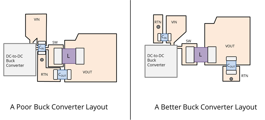
Figure 4: Two possible board layouts for a buck converter.
You may be thinking that the layout on the left is so obviously bad that nobody would ever attempt something like this. But similar layouts appear in many vendor application notes and datasheets. In general, you shouldn’t rely on EMC layout recommendations from power converter vendors. Many of them are based on rules that were developed many years ago when switching frequencies were lower, and components were much larger.
In most cases, simply controlling the surface area of the switching voltage node and the loop area of the switching current loop is sufficient to keep high-frequency switching currents from spreading to other parts of the board or system. However, there are additional design options that can be useful in situations where the layout alone doesn’t limit the coupling sufficiently. For example, most converter vendors offer low-noise options such as spread-spectrum clocking and building the CIN capacitor into the IC. Low-noise converters may also offer a more thoughtful placement of their I/O pins to facilitate an optimum layout.
Boost Converters
Boost converters are used in situations where it is necessary for the output DC voltage to be higher than the input DC voltage. The basic boost converter topology is illustrated in Figure 5. Like the buck converter, the boost converter employs a switch and a diode (or two switches for a synchronous boost converter). The inductor is on the input side of the converter. Closing the switch in Figure 5 causes current to flow through the inductor. Once a sufficient current has been reached, the switch opens, causing the voltage on the switching node to jump to the value of the input voltage plus L dI/dt. With the switch open, this voltage starts to drop as current flows to the load. Closing the switch sends the voltage on the switching node to zero, but the diode and capacitor prevent the voltage across the load from dropping rapidly. Meanwhile, with the switch closed, the inductor builds up stored energy, and the cycle is repeated.

Figure 5: DC-to-DC boost converter topology.
Like buck converters, boost converters usually operate at a fixed frequency and use pulse-width modulation to control voltage at the output. Like buck converters, they have a switching voltage node and a switching current loop. The key to a good boost converter layout is controlling the electric-field coupling from the switching voltage node and the magnetic-field coupling from the switching current loop.
Figure 6 shows two possible boost converter layouts. The layout on the right resembles the buck converter layout in Figure 4 with VIN and VOUT swapped. The switch node is reasonably small and isolated. The switching current, which flows from the IC through COUT and back on the RTN plane, is a relatively small, isolated loop.
The layout on the left uses a PGND trace to carry the switching current back to the IC, where it makes a single-point connection to the IC GND pin and the RTN plane. Isolated power current returns like this are reminiscent of the days when power converters switched at kHz frequencies. Back then, the switching currents were a source of common-impedance coupling to other circuits sharing the same “ground.” With switching frequencies now routinely in excess of 100 kHz, common-impedance coupling is no longer a problem on boards with a solid return plane. The high-frequency switching current stays largely confined to the small region of the plane directly below the components. It minimizes its own loop area. Providing an isolated PGND plane, as shown in the figure, is not only unnecessary, but it also increases the inductance of the loop.
Another mistake in the layout on the left is that the CIN capacitor connects to the PGND. This creates a significant mutual inductance between the switching current loop and VIN. With this layout, switching noise will be strongly coupled to the input voltage and eventually back to the board’s power supply.
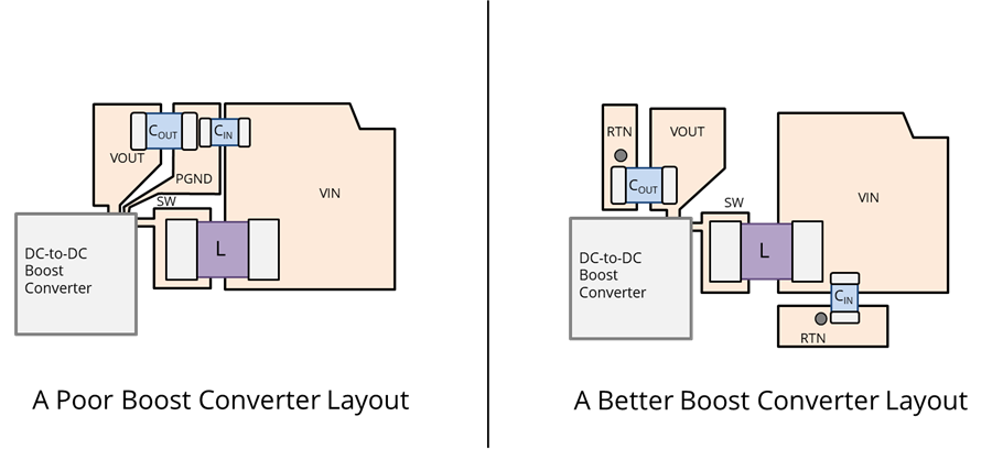
Figure 6: Two possible board layouts for a boost converter.
The layout on the left appears to be designed to maximize conducted and radiated emissions. It is a terrible layout. Nevertheless, it is based on design advice that can be found in a number of application notes and datasheets.
H-Bridge Inverters
An H-bridge can produce voltages with a positive or negative polarity. They are often used to drive DC motors both forward and backward. They are also capable of taking a DC input voltage and producing an AC output, so they can be used to drive AC motors as well.
An H-bridge inverter employs four switches as illustrated in Figure 7. When the switches on the upper-left and lower-right are closed, current flows to the load on the upper wire and returns on the lower wire. The amount of current can be regulated by pulse width modulation. Typically, the upper switch is modulated while the lower switch remains closed.

Figure 7: H-bridge inverter topology.
To achieve a negative voltage across the load, the switches on the upper-right and lower-left are closed. Now, current flows to the load on the lower wire and returns on the upper wire. This current can also be regulated using pulse width modulation. Figure 8 illustrates how pulse width modulation of the positive and negative voltages can be used to produce a sinusoidal current flowing to the load.
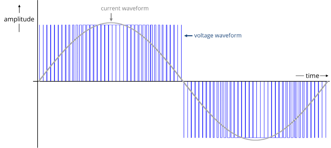
Figure 8: PWM representation of a sine wave.
An H-bridge converter has two switching voltage nodes, the connections between the upper and lower switches. Unlike buck and boost converters, the switching voltage nodes in an H-bridge converter carry current away from the inverter. We can’t limit the noise by simply keeping their area small and far from other circuits. However, since the intentional current flowing to the load is relatively low-frequency, it is easy to filter the conductors connected to these nodes. In many cases, it is also possible to control the transition time of the switches to limit the higher harmonic content of the switched power. And in situations where filtering is not practical, shielding of the inverter, cable and load can be used to limit the electric-field coupling.
There are effectively several switching current loops in an H-bridge. All the switches have a capacitance when they are open, so high-frequency current can flow from the high-side voltage through any pair of high-side and low-side switches to the low-side voltage, then return to the high-side voltage through any other pair of switches or through the input capacitor (CIN in Figure 7). To reduce magnetic field coupling from the inverter circuitry, it is important to keep these loop areas small and isolated from other circuits that could carry the coupled voltage away from the inverter.
Figure 9 illustrates two possible board layouts for an H-bridge motor driver. This design uses switches that require mounting along the board edge to facilitate thermal heatsinking. Both layouts include a filter on the motor output. Both layouts keep the motor-driving circuitry away from the digital control circuitry. However, the layout on the left has connectors on opposite sides of the board. This allows the voltage that develops across the return planes to drive one cable relative to the other. To make matters worse, the reference for the cable connecting to the motor is different from the reference for the cable on the right because the layout uses an isolated motor “ground.”
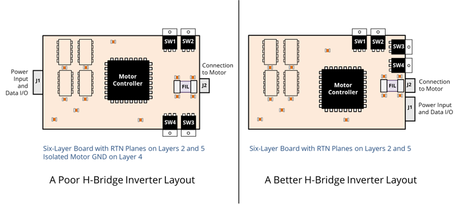
Figure 9: Two possible board layouts for an H-bridge inverter.
The layout on the right puts both I/O connectors near each other, while still maintaining reasonable isolation between the digital circuits and the motor-driving circuits. It does not have an isolated motor ground, which would rarely be required in applications like this. Since this board is mounted to a large heatsinking structure, the board RTN planes should be connected to that structure along the edge with the external connections.
Flyback Converters
Flyback converters are typically used in situations where it is necessary to isolate the current return paths on each side. A common example of this is a power supply that plugs into a wall outlet. In this case, the input voltage is high enough that none of the power current is allowed to flow on the chassis. On the other hand, it is usually advantageous to connect the current return on the low-voltage side to the chassis to meet EMC requirements.
The basic topology of a flyback converter with its secondary grounded is illustrated in Figure 10(a). Galvanic isolation between the input and the output is provided through a transformer. The primary side of the transformer is connected to the voltage source through a switch. As the primary side current is switched on and off, a voltage appears on the secondary. This voltage can be higher or lower than the primary side voltage, depending on the transformer’s turns ratio. The power on the secondary side is rectified to provide a DC voltage across the load,
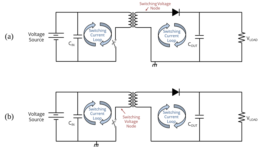
Figure 10: Flyback converter topology.
The topology in Figure 10(b) is identical to that in 10(a) except the primary side is grounded and the secondary side is not. This would be common in situations where a relatively low voltage was stepped up to a very high voltage. From a layout standpoint, one difference between the two topologies is the location of the switching voltage node. From an electric-field coupling standpoint, we are most concerned with voltages that rapidly change relative to the ground structure. So even though the switch is on the primary, the switching voltage node on the secondary in Figure 10(a) should not be overlooked.
The voltage across the switch in Figure 10(a) can also be a source of electric-field coupling, so it is important to pay attention to the layout on the floating (primary) side of the converter as well. In most cases, since neither the power nor the power-return conductors are ground, it is best to have them mirror each other with neither conductor being substantially larger than the other. In other words, the power distribution on the floating side should be balanced.
In situations where the floating side is unbalanced (e.g., the power is routed on a trace and the power-return is routed on a plane), then the plane conductor should make a good high-frequency connection to the ground. In this case, both sides are considered to have the same high-frequency ground, and the node on the other side of the switch is another switching voltage node.
The same reasoning applies to Figure 10(b), where the primary side is connected to ground. In this case, the secondary side should normally be balanced. However, when the secondary side is not balanced, its current-return should have a good high-frequency connection to the ground structure.
Flyback converters have two high-frequency switching current loops, as indicated in Figure 10. When laying out flyback converters, it is important to minimize the area of these loops to prevent magnetic-field coupling to other circuits.
Figure 11 illustrates an example of a good flyback converter layout. In this example, power from a wall outlet is converted to a low DC voltage that powers the rest of the board. There is a solid return plane on Layer 2. The primary power does not connect directly to the plane, but it is filtered using X and Y capacitors as well as a common-mode choke. The input switching current loop (connector to switch to transformer and back to the connector) is kept reasonably small and away from other circuits. The output current loop (transformer to diode to capacitor to ground and back) is also minimized and doesn’t couple readily to any other circuit. The switching voltage node (the connection between the transformer and diode) is very small.
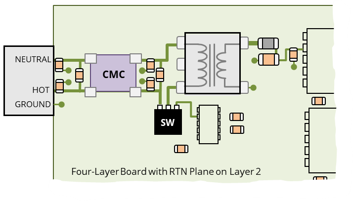
Figure 11: A good flyback converter layout.
Other applications may call for very different layouts, but the emphasis should always be to minimize coupling from the switching voltage nodes and switching current loops that could carry noise away from the immediate area. The layout in Figure 11 has all the components on the top side of the board. In general, both sides of the board can be utilized in power converter designs as long as the switching current loops do not pull current through the board. In this design, the transformer, the switch, CIN, COUT, and the diode should all be on the same side. On the other hand, the filter components and control circuitry could be mounted on the top or the bottom. The location of these components should be chosen to optimize their performance while minimizing any unwanted noise coupling.
Inverting Buck-Boost Converters
The four power circuit topologies described in the previous sections (buck, boost, H-bridge, and flyback) have the essential building blocks found in many other common topologies. Once you are comfortable identifying the switching voltage nodes and switching current loops in these power circuits, it is relatively straightforward to identify the same features in other power circuit topologies.
For example, consider the inverting buck-boost converter whose basic topology is illustrated in Figure 12. This circuit is commonly used to convert a positive DC input voltage to a negative voltage across the load. In order to identify the switching voltage node, we look for the connection to the switch that is shared with the inductor (just as it is in a buck or boost converter). To identify the switching current loop, we start with the switch and find the lowest-impedance high-frequency path that completes the loop. The switching current path always involves at least one switch, but it never flows through an inductor. In Figure 12, we see that the switching current loop flows through the switch, diode, COUT and CIN.

Figure 12: Inverting buck-boost converter topology.
Like other power circuit topologies, a good layout minimizes the electric-field coupling from the switching voltage node and the magnetic-field coupling from the switching current loop. Figure 13 shows two possible inverting buck-boost converter layouts. In this case, the switch and diode are located inside the IC with the control circuitry. As in the previous examples, Layer 2 is a solid return plane.
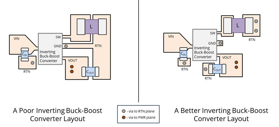
Figure 13: Two possible board layouts for an inverting buck-boost converter.
In the layout on the left side of Figure 13, the switching voltage node is larger than it needs to be. It couples to a return trace on the top layer that only makes a single-via connection to the plane on Layer 2. Depending on what is located nearby, this could allow electric field coupling to carry noise away from the converter.
A bigger problem with the layout on the left in Figure 13 is that the switching current loop is much too large. If we trace it from VIN through the IC to VOUT and through COUT, it must flow across the return trace on Layer 1 to the via, then to the plane to get to CIN and back to VIN. This large loop facilitates magnetic-field coupling to nearby circuits.
The layout on the right of Figure 13 minimizes the surface area of the switching voltage node and minimizes the loop area of the switching current loop. Note that, for this converter, the switching current between CIN and COUT stays on the plane. It does not need to return to the GND pin of the IC. As a rule, for any of the converter layouts we’ve discussed, if there is a solid return (or GND) plane on Layer 2, return (or GND) traces are not required or helpful on Layer 1. All RTN or GND connections should be made directly to the plane.
Other Power Circuit Topologies
As previously indicated, other common power circuit topologies have the same elements found in the buck, boost, H-bridge, and flyback topologies. Figure 14 illustrates a SEPIC (Single-Ended Primary-Inductor Converter) topology, which is basically a non-inverting buck-boost converter. These converters can step a DC voltage up or down. This topology has two switching voltage nodes and one switching current loop.
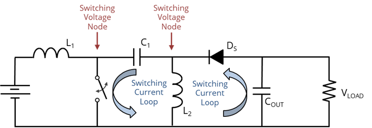
Figure 14: SEPIC converter topology.
Figure 15 shows the basic topology of an active-clamp forward converter. It utilizes elements found in the flyback and buck converters. Active-clamp forward converters can step DC voltages up or down and are often used in high-power applications. These converters are isolated like flyback converters, and the location of the switching voltage nodes depends on which side(s) of the inverter is (are) connected to ground. The locations in the figure assume the lower node on both sides is ground. This topology has three switching current loop areas to minimize.
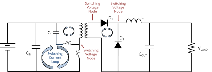
Figure 15: Active-clamp forward converter topology.
Figure 16 shows the basic topology of a three-phase inverter. It’s basically an H-bridge inverter with an extra phase output. Three-phase inverters are widely used for driving medium-to-high-power variable-speed AC motors. Like an H-bridge inverter, each of the outputs is a switching voltage node and should generally be filtered or shielded if it extends very far from the switches. There are also multiple switching current loops whose area should be minimized.

Figure 16: Three-phase inverter topology.
If shielding is required on the wires between the inverter and the load, all of the wires should be inside the same shield. Shields on individual wires are forced to convey relatively strong differential switching currents. Any small impedance in the shield’s connection to the ground structure can then result in a voltage that drives the cable shields relative to the structure. On the other hand, a shield around all three wires only carries the relatively small current associated with any unintentional common-mode voltage driving the wires.
Snubber Circuits
The switching voltage node of a power circuit sees a very high dV/dt. In many cases, the voltage on this node overshoots its target and rings as depicted in Figure 17. This ringing is generally associated with the inductance of the switching current loop and a capacitance in the loop (usually an open switch capacitance). In the frequency domain, this ringing appears as a relatively narrow-band peak in the coupled noise.
The energy that drives this ringing typically comes from two sources. The first is the energy stored in the magnetic field associated with the switching current loop. This is proportional to the inductance of the loop and the square of the current flowing in the loop. The second source of ringing energy is the reverse recovery current injected into the loop when a conventional MOSFET or IGBT switch transitions from a closed to an open state. Reverse recovery current is due to a brief injection of charge that results when a diode transitions from a forward bias to a reverse bias. It can be the primary driver of ringing in power circuits employing conventional silicon switches. On the other hand, wide band gap switches (e.g., GaN or SiC devices) have virtually no reverse recovery current.

Figure 17: Ringing in a voltage waveform.
One method to reduce ringing in a switch node is to apply a snubber circuit across the switch (or between the switching node and circuit ground). In most cases, the snubber circuit is a small resistor in series with a capacitor. Snubber circuits applied to an H-bridge inverter are illustrated in Figure 18.
Figure 18: Snubber circuits applied to an H-bridge inverter.
Linear Voltage Regulators
Finally, no discussion of power circuit layout for EMC would be complete without mentioning linear voltage regulators. Linear voltage regulators convert one DC voltage to another (lower) DC voltage by essentially forming a voltage divider that shunts excess current to ground. They are only used when the difference between the source voltage and output voltage is relatively small, because shunting a lot of current to ground wastes power and generates heat. On the other hand, compared to switching power converters, they are small and inexpensive. Most importantly, from an EMC perspective, they don’t produce any switching noise.
References
[1] M. Zehendner and M. Ulmann, Power Topologies Handbook, Texas Instruments, 2020.