
Chapter 11 Exercise: Visual Inspection of Circuit Boards
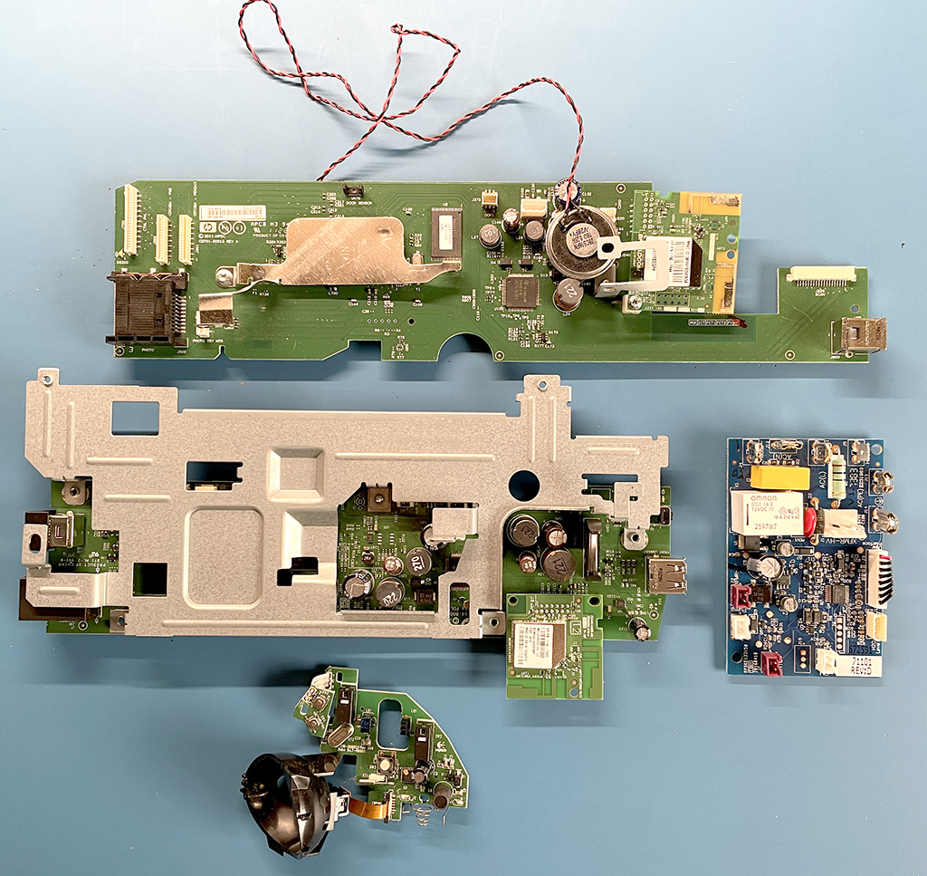
This lab gives students a chance to apply things they've learned about designing for EMC to actual products.
Preparation: Students should read Chapter 11 of the book, including the suggested steps for reviewing a printed circuit board layout. The boards reviewed in this lab can be salvaged from broken or no-longer-needed computing devices, including laptops, printers, routers, and appliances.
Equipment Required:
- a selection of 3-5 printed circuit boards taken from commercial electronic devices
- ohm meter
- magnifying glass
Procedure:
Step 1: For each board, students working in groups of 2 or 3 are asked to identify:
- the EMC tests and requirements the product was (most likely) subjected to
- the location of the EMC ground(s)
- the location of relevant test ports/antennas
- the locations of relevant components (e.g. decoupling or filter capacitors, inductors, ferrites ...)
Step 2: Students should comment on potential problems with the layout; what was not done well and what kind of EMC problem might arise as a result.
Step 3: A visual inspection of a board doesn't reveal all of the information necessary to do a good design review. Students should comment on anything they would look for in the stack-up or the schematics that would be relevant to their recommendations.
Notes:
It's a good idea to review one or two designs in class before students do the lab exercise. Students will get better at this with every new review.
This is generally one of the most popular labs in an EMC course. However, its success depends on having a variety of circuit board designs to review. After the labs have been turned in, it's helpful to have a class discussion about the various features identified by different groups.