Electromagnetic Compatibility Course Notes - Supplement
This page is a repository for supplemental information related to the book Electromagnetic Compatibility Course Notes. It will be updated with error corrections, content updates, problem solutions, and links to information related to the material presented in the book.
In each section, click on the ▶ to expand the text.
Errors and Corrections
Please report errors to
Chapter 7 - page 189.
The book says, "However, equal and opposite currents on an unbalanced wire pair are inconsistent with differential-mode propagation." This is not strictly correct. Equal and opposite currents on an unbalanced wire pair imply the existence of a common-mode voltage, but are still consistent with differential-mode propagation.
The following sentence says, "Both differential and common-mode propagation are required." Since this example is a two-wire transmission line, the common-mode is not a propagating mode. The common-mode voltage drives a common-mode current on the line. That current can result in radiated emissions, but it is not associated with a propagation mode.
Problem Solutions
Chapters 1-3
Chapter 1 - Solutions
1. For each of the EMC problems below, identify the probable source,
coupling path and receptor.
a.) Source: Microwave Oven, Coupling Path: Radiated Field, Receptor: Computer Display
b.) Source: Starter Motor, Coupling Path: Conducted (through power wiring), Receptor: Car Radio
c.) Source: Lightning, Coupling Path: Conducted (Power or Communication Wiring), Receptor: Modem
d.) Source: Blanket, Coupling Path: Radiated (likely) or Conducted through Power Wiring, Receptor: WiFi Router or Device
e.) Source: Airport Radar or Transmitter, Coupling Path: Radiated Field, Receptor: Tire Pressure Monitoring System
2. What are alternative names for conducted, inductive, and capacitive coupling?
Conducted Coupling ⇒ Common Impedance Coupling
Inductive Coupling ⇒ Magnetic-Field Coupling
Capacitive Coupling ⇒ Electric-Field Coupling
3.
4. 150 mV = 43.5 dB(mV) = 104 dB(μV) = –3.5 dBm
5. 6 dB (same as ratio of rms amplitudes)
6. +12 dB - 6 dB = +6 dB (or a factor of 2 in voltage), so output amplitude is 2 volts.
7. The term 50% gain is ambiguous. Does it mean 50% of the original amplitude (factor of 0.5) or 50% more (factor of 1.5)?
By the first interpretation, answers are 0.5 V, 1 V, 2V and 5V. By the second interpretation, answers are 1.5 V, 2 V, 3 V and 6V. These answers would all be different, if we interpreted the 50% gain to be a power gain instead of a voltage gain. Note that a 100% gain is generally interpreted as a doubling of the amplitude. However, a 200% gain is also generally considered a doubling of the amplitude. Signal gains, losses, or error margins should usually be expressed in dB in order to avoid misinterpretation.
8. 46 dB(μV/m) - 40 dB(μV/m) = 6 dB. Note that it is NOT 6 dB(μV/m), which is a signal amplitude totally unrelated to the correct answer.
9. 200 μV/m = 46 dB(μV/m). 100 μV/m = 40 dB(μV/m). 46 dB(μV/m) - 40 dB(μV/m) = 6 dB. Note that we could also say that the measured field is 200 μV/m - 100 μV/m = 100 μV/m over the limit. In most cases, however, it will be more helpful to know the ratio in dB rather than the difference in the field strengths.
10. Bulk Current Injection is an immunity test.
11. Radiated Immunity and Bulk Current Injection testing should be done in a shielded room to contain the fields and prevent them from interfering with the test equipment and other nearby electronic devices. Some radiated emissions tests also specify an absorber-lined shielded room, although useful emissions measurements could still be made outside the room. A shielded room is not required for conducted emissions and transient immunity measurements.
12. Conducted Emissions, Bulk Current Injection, Lightning Immunity and Electrical Fast Transient Immunity tests can only be done on products with an attached cable.
Chapter 2 - Solutions
1. @ DC: R ≈ 170 mΩ/m. @ 1 MHz: R ≈ 330 mΩ/m. @ 1 GHz: R ≈ 10 Ω/m.
2. C ≈ 52 pF/m
3. L ≈ 52 nH/m
4. At DC, we'll assume that the plane resistance is negligible relative to the trace resistance. The trace resistance is 4.0 Ω/m or 40 mΩ/cm.
At 10 MHz, the plane current is focused under the trace, so we'll assume that the plane resistance is approximately equal to the resistance of the trace. Skin depth is 21 μm, which is slightly thicker than the half-ounce copper. Resistance of the trace is still about 40 mΩ/cm. Resistance of the trace and plane is about 80 mΩ/cm or a little less.
5. C/ε = G/σ therefore G = C(σ/ε) = (10-10 F/m x 5.4 x 10⁻⁴ S/m) / (4.3 x 8.854 x 10-12 F/m) = 0.0014 S/m (or 1.4 x 10⁻⁵ S/cm).
6. Inductance of each loop is 0.146 μH. Leakage inductance is approximately the inductance per unit length of the wire pair (edge-to-edge spacing is 0.5 mm) times the circumference of the loop. This is 0.52 μH/m x 0.16 m = 0.083 μH. So mutual inductance is approximately 0.146 - 0.08 = 0.066 μH. Note that his is a coupling coefficient of only k = 66/146 = 0.45 (about 45%). Even though the loops share a lot of area, most of the flux is near the wire and the wire-to-wire spacing is too large to get efficient coupling. Using the same method, reducing the wire insulation thickness to 0.025 mm would increase the coupling coefficient to 80%.
7. Due to the symmetry of the wire cross-section, the mutual inductance must be half the self-inductance of the circuit using wires 1 and 3. The self-inductance of that circuit is 0.92 μH/m x 0.5 m = 0.46 μH. The mutual inductance is therefore 0.23 μH.
8. The impedance of a 1-μF capacitor is less than 5 Ω at frequencies above 1/2πRC = 31.8 kHz. A 5-nH inductor has an impedance less than 5 Ω at frequencies below R/2πL = 159 MHz. Therefore, the range of frequencies where the capacitor's impedance is less than 5 Ω is about 32 kHz to 160 MHz.
9. The impedance of a 2.2-μF capacitor is less than 5 Ω at frequencies above 1/2πRC = 14.5 kHz. A 5-nH inductor has an impedance less than 5 Ω at frequencies below R/2πL = 159 MHz. Therefore, the range of frequencies where the capacitor's impedance is less than 5 Ω is about 14.5 kHz to 160 MHz.
10. At DC, the ground strap impedance is its resistance: R ≈ 0.35 mΩ. At 10 kHz, the resistance is about the same and the inductance (from Equation 2.32) is about 460 nH, which is an impedance of about 29 mΩ. The inductance dominates, so the ground strap impedance is 29 mΩ. At 10 MHz, the inductance is still 460 nH, so the ground strap impedance is about 29 Ω.
Chapter 3 - Solutions
1. At DC, the resistance of the 20-meter return wire is 1.68 Ω. The source current is VS1 / 100 Ω, so the voltage dropped across the return conductor is VS1 x 1.68/ 100 Ω = 0.0168 VS1.. The portion dropped across the victim circuit load is (100/110) x 0.0168 VS1., so the ratio VS2/VS1 is 0.0153 or -36 dB.
At 1 MHz, the resistance of the 20-meter return wire is 3.25 Ω. All other values are the same as they were at DC. Therefore, the coupled voltage is a factor of 3.25/1.68 higher. This is 0.030 or -31 dB.
At 3 MHz, the resistance is 5.63 Ω. The coupled voltage is a factor of 5.63/1.68 higher than at DC. This is 0.051 or -26 dB.
2. The mutual capacitance is 52 pF/m x 20 m = 1.04 nF. At DC, there is no capacitive crosstalk. Using Equation 3.11, the crosstalk at 1 MHz is -23.7 dB. At 3 MHz, it is a factor of 3 higher or -14 dB.
3. The mutual inductance is 200 nH/m x 20 m = 4.0 μH. At DC, there is no inductive crosstalk. Using Equation 3.40, the calculated crosstalk at 1 MHz is -12 dB. At 3 MHz, simply assuming the crosstalk is a factor of 3 higher yields a crosstalk value of -3 dB. This value suggests the weak coupling assumption has been violated. We do not have enough information to calculate the crosstalk precisely; however, the self-inductance of the source loop must be greater than 4.0 μH. At 3 MHz, this is 75 Ω and is nearly has high as the load resistance. In other words, the signal is significantly distorted, and the precise value of the crosstalk is probably irrelevant.
4. Changing the receiver impedance from 100 Ω to 1 MΩ drops the current in the source circuit to near zero. The common-impedance coupling is virtually eliminated (-115 dB @DC, -110 dB @1 MHz, -100 dB @3 MHz). The inductive coupling is also virtually eliminated (-92 dB @1 MHz, -82 dB @3 MHz).
The only significant coupling is due to capacitive coupling, which is non-existent at DC, but is still -23.7 dB @1 MHz and -14 dB @3 MHz.
5. The resonant dipole input resistance is approximately 72 Ω. Source voltage is 1 mVrms. Therefore, the power delivered to the dipole and radiated is approximately 14 nW.
6. Power density in the direction of maximum radiation is Prad (D0/4πR2) where the dipole directivity, D0, is 1.6. So, the maximum power density is 200 pW/m2. This corresponds to a field strength in free space of about 270 μV/m. In a semi-anechoic environment, the field strength will be doubled in places where the source and its image create fields that add in phase. This means the maximum field strength in a semi-anechoic environment will be 540 μV/m.
7. The differential-mode current is (1 v) / (102 Ω) = 9.8 mA. Using Equation 3.62, the radiated field strength at 3 meters is 43 μV/m.
8. Here's one example. Length is 1.3 meters. Length of a half-wave dipole at 20 MHz is 7.5 meters.
9. Since log-periodic arrays have elements that are approximately a half wavelength long, these antennas would be very large. They would be essentially unusable at heights of 1-meter above a ground plane as required for most radiated emissions measurements.
10. Due to the skin-effect, thin wire antennas start to become pretty lossy at GHz frequencies. The smallest elements of a log-periodic array need to be fairly closely (and precisely) spaced. This does not work well with thick elements. Horn and patch antennas don't have thin wires and tend to work better at GHz frequencies.
Chapters 4-6
Chapter 4 - Solutions
1. a.) In peak detection mode, the spectrum analyzer measures the peak rms value of the signal, which is 1.41 volts or 16 dBm.
b.) The signal is continuous with constant amplitude, so the quasi-peak and peak values are the same, 16 dBm.
c.) The signal is continuous with constant amplitude, so the average and peak values are the same, 16 dBm.
2. The first harmonic of a square wave has an rms amplitude that is 0.45 times the peak-to-peak value. In this case, 0.9 volts or 12 dBm @ 1 MHz. The third harmonic is one-third of this value, 0.3 or 2.55 dBm. The 15th harmonic is 60 mV or -11.4 dBm. The 35th harmonic is 26 mV or -19 dBm.
3. A 40-ns transition time places the second knee frequency at 8 MHz. The amplitudes of the harmonics at 1 MHz and 3 MHz are not changed much. The amplitudes of each harmonic calculated using Equation 4.16 to get the peak amplitude and then multiplying by 0.707 to get the rms amplitude are:
1 MHz — 0.9 volts or 12 dBm (same as square wave)
3 MHz — 0.29 volts or 2.3 dBm (-0.35 dB compared to square wave)
15 MHz — 0.03 volts or -17 dBm (-5.6 dB compared to square wave)
35 MHz — 0.0056 volts or -32 dBm (-13 dB compared to square wave)
4 and 5. Plot shown here.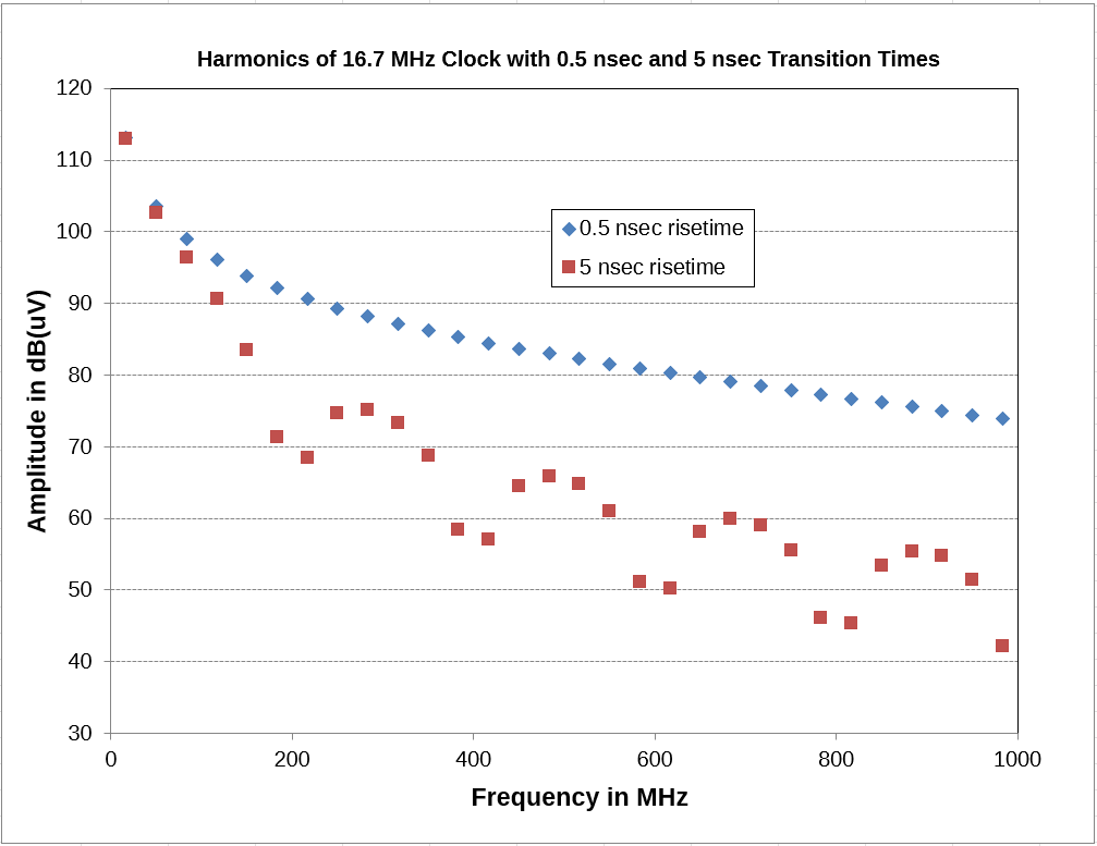
6. Plot shown here.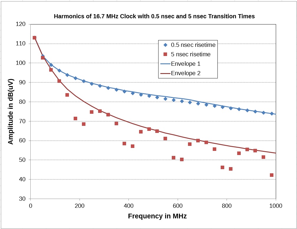
7. 1.4 mV or -88 dBm.
8. Noise power is proportional to resolution bandwidth. Reducing bandwidth by 9/120 reduces noise floor by 10 Log (9/120) = -11 dB. So new noise floor is at -91 dBm.
9. (a.) FFT BW = 1/fs. Displayed bandwidth (one-sided) BWmax < 1/2 x 109) = 500 MHz.
(b.) Δfres = 1/T = 125 kHz.
(c.) To get better frequency resolution, it's necessary to sample more of the input signal.
10. As indicated in Figure 4.13, the quasi-peak attack time constant is 1 ms and the decay time constant is 160 ms. So any signal that is present for 2.2 ms and doesn't go away for substantially longer than 2.2 ms will not have a quasi-peak value significantly lower than the peak value. Therefore, pulses occurring at a rate of 15 kHz, 100 kHz, and 1 MHz will have quasi-peak values approximately equal to their peak values. Pulses occurring with a repetition rate of 60 Hz (period of 17 ms) would be expected to have a quasi-peak value less than the peak value.
Chapter 5 - Solutions
1. The velocity of propagation is 3x10⁸/sqrt(4.3) = 1.45x10⁶ m/s. The propagation delay is length/velocity or about 690 ps.
2. 
3. C = 100 pF/m and LC = με, so L = με/C = 478 nH/m. Z0 = sqrt(L/C) = 69 Ω.
4. The reflection coefficient for the forward-traveling wave only requires a load end. If the transmission line is matched at the load end, there are no reflections.
5. Increasing the width of a circuit board trace means,
(a.) Characteristic impedance decreases.
(b.) Inductance per unit lengths decreases.
(c.) Capacitance per unit length increases.
(d.) Propagation delay stays the same for a stripline, decreases slightly for a microstrip line.
(e.) Resistance per unit length decreases.
(f.) Conductance per unit length increases.
6. Cable properties
(a.) Inductance per unit length: 630 nH/m
(b.) Capacitance per unit length: 51 pF/m
(c.) Resistance per unit length: 325 mΩ/m
(d.) Characteristic impedance: 111 Ω
(e.) Propagation velocity: 1.76 x 10⁸ m/s
(f.) Cable attenuation at 1 MHz: (from Eqs. 5.31 and 5.32) 12.7 dB/km.
7. For the transmission line in the problem statement,
(a.) Γ = 0.41
(b.) VSWR = 2.4
(c.) At 250 MHz, the cable wavelength is 80 cm. βl = 1.25π. tan(βl) = 1.0. Zin = 50 (120 + j50)/(50 +j120) = 35.5 + j35.2 Ω.
(d.) Magnitude of current in = 3.3/|40.5 + j35.2| = 0.061 amps. Power in is Pin = I2Rin = 134 mW. Line is lossless, so all of Pin is delivered to the load.
(e.) V = sqrt(Pin x R) = sqrt(0.134 x 120) = 4.0 Vrms. (Note that the load voltage is higher than the open-circuit source voltage.)
8. From Eq. 5.50, Leq = 5.1 nH.
9. The fields above and below the trace must travel together. Their velocity is slower than a plane wave traveling in air, but faster than a plane wave traveling entirely in the dielectric.
10. The only meaningful voltages in an RLCG model are the differential voltages between the two conductors at any position along the length. Any voltage differences between points at two different locations along the length of the transmission line are artifacts of the calculation. They do not correspond to meaningful voltage differences that could be measured on a real transmission line. In fact, voltage differences along the length of the line are not uniquely defined.
Models that put resistances and inductances on both sides of the RLCG equivalent, are unnecessarily complex. But worse, they imply that there is a unique and calculable voltage difference between the reference on one end of the line and the reference on the other end.
Chapter 6 - Solutions
1. Applying the circuit model in Fig. 6.3 and making the weak coupling assumption,
(a.) IC = C dV/dt = (3 pF) (3.3 V)/(2 ns) = 5 mA. Multiplying by the parallel combination of the victim circuit impedances, Vcoupled = 10 mV. So, the coupled waveform is a positive or negative 2-mV pulse that lasts 2 ns that occurs with each signal transition. Note that the 5 pF load draws a current of C dV/dt = (5 pF) (2 mV)/(~1 ns) = 10 μA. This is much less than the 5 mA in the source resistance, so the load capacitance doesn't significantly affect the coupled voltage.
(b.) Terminating with a 50-Ω resistance would have little effect on the coupling in this case, because 50 Ω is still large compared to 2 Ω.
2. Moving the traces farther apart decreases C12 and slightly increases C11 and C22.
3. Moving the traces farther apart decreases L12.
4. The 50-Ω scope impedance and C12 form a voltage divider with 7.5 mV dropped across the 50 Ω. The current through 50-Ω scope resistance is 7.5 mV/50 Ω = 150 μA. Therefore, the impedance of C12 is approximately (1 V)/(150 μA) = 6.67 kΩ. At 1 MHz, this is a capacitance of C12 = 24 pF or 12 pF/m.
5. The current in the source circuit is (1 V)/(50 Ω) = 20 mA. The coupled voltage is ωM12I = .45 V. Therefore, M12 = 3.6 μH or 1.8 μH/m.
6. Below 100 kHz, the coupling would be very weak, and the coupled voltages would be hard to measure accurately. At frequencies much higher than 10 MHz, the 2-meter cable is no longer electrically short and doesn't have a constant voltage or current along its entire length.
7. A copper wire with a 1-mm diameter has a DC resistance of 21 mΩ/m. A 100-meter wire has a resistance of about 2.1 Ω. Carrying 8 A of current, the voltage drop across the wire would be about 17 volts. Since the sensor uses the same return wire, the sensor circuit would see this 17 volts whenever the motor started.
8. At these frequencies, the cable is electrically long. The maximum near-end crosstalk is 20 Log[C12/(C22+C12)] = -11 dB. At frequencies above 1 GHz, the wires will be lossy enough that the signal amplitudes and crosstalk will start to be attenuated.
9. Note that the end-to-end propagation delay for the cable is 53 ns. At 5 Mbps, the 10-meter cable is not electrically long. However, it is long relative to a transition time of 20 ns. Therefore, the coupled near-end voltage is a pulse with a maximum amplitude of (ΔV/2) x [C12/(C22+C12)] ≈ 170 mV. The pulse duration is 40 ns. Positive then negative pulses are coupled with every signal transition.
10. At 200 Mbps, the cable is electrically long. The maximum coupled voltage at the near end is still 170 mV but the coupled waveform has a shape similar to the signal waveform.
Chapters 7-9
Chapter 7 - Solutions
1. With a 1-ns transition time, the 2nd knee frequency is 318 MHz (well above 35 MHz). Amplitude of first harmonic is 0.45 x 3.3 volts = 1.5 volts. Amplitude of 35th harmonics equals 1.5/35 = 42 mV. At the connector, the transition from unbalanced to balanced creates a common-mode voltage equal to half the signal voltage (i.e., 21 mV).
2. Without a change in the imbalance, there is no common-mode voltage generated.
3. h = C11/(C11+C22) = 0.4. Note that labeling the wider trace as conductor 1 would give a value of 0.6. Either value of h describes the same level of imbalance.
4. VCM = Δh x VDM = (0.4 - 0.5) 42 mV = -4.2 mV. (or +4.2 mV if the wider conductor is conductor 1). The polarity of VCM only becomes important when there are multiple imbalance changes in the same signal path. In that case, it's only necessary to be consistent with the definition of conductor 1 (keeping it on the same side of the signal).
5. Using ATLC2, h ≈ 0.33 (or, 0.67 depending on which conductor was labeled conductor 1).
6. Using the same procedure used in Example 7-4, the propagation velocity is 3 x 10⁸ m/s, CDM is 24.5 pF/m. LDM is therefore 454 nH/m. k = 0.531. Applying Eq. 7.13 and 7.18, L11=L22 = 0.48 μH/m. L12 = kL11 = 0.26 μH/m.
7. Using the procedure used in Example 7-5, ZDM = 142 Ω and ZCM = 98 Ω. Z1 = 196 Ω and Z12 = 173 Ω.
8. The percentage of the differential-mode signal that drives the cable relative to the plane is zero. Both the differential-mode source and transmission lines are balanced, so there is no mode conversion. The percentage of the common-mode source voltage that drives the ribbon cable relative to the plane is close to 50%. The common-mode propagation on the board is very unbalanced (out on two traces and back on a wide plane). The common-mode propagation on the cable is nearly balanced (out on two wires and back on two wires). Approximately half of the common-mode voltage drives the cable, and the other half is converted to differential-mode.
9. Because common-mode and differential-mode propagation are independent, they can travel at different velocities. Single-ended signals have only one propagation mode, so they are not affected by this. Differential-mode signals only propagate in the differential-mode, so they are not directly impacted. However, if there is a common-mode component of the source voltage (e.g., as generated by pseudo-differential drivers), then the common-mode noise pulses travel with a different velocity.
10. Perhaps the main reason circuit designers don't take advantage of orthogonal propagation modes is the complexity involved in generating and receiving independent common-mode and differential-mode signals. Yes, it can be done, but at most practical transmission line lengths, the crosstalk is a relatively minor issue and doesn't warrant added cost or complexity in the source or receiving circuits. Another consideration is that maintaining perfect balance can be difficult, especially as signals propagate through connectors. And some crosstalk would occur in the driver and receiver circuitry. So, utilizing orthogonal propagation modes doesn't solve the crosstalk problem, it just redefines it.
Chapter 8 - Solutions
1. For each of the conductors commonly labeled ground listed below, indicate whether it is a safety ground, EMC ground, or current return.
(a.) Ground wire in building electrical distribution wiring (safety)
(b.) Frame ground in an electric oven (safety and EMC)
(c.) Frame ground in an automobile (EMC > 1 MHz, current return for <48 V and < 1 MHz, safety ground for >48 V in electric vehicles)
(d.) Frame ground in a large commercial aircraft (safety and EMC)
(e.) Frame ground in a cell phone (EMC)
(f.) Circuit board signal ground plane (current return)
(g.) Circuit board chassis ground plane (EMC)
(h.) Ground plane in an EMC test setup (EMC)
(i.) Coaxial cable shield (EMC and current return)
2. EMC grounds are mostly utilized at high frequencies (e.g., > 1 MHz). Intentional low-frequency currents in a product's frame ground generally don't create enough of a voltage to cause an EMC problem.
3. Common-impedance coupling can be a problem when a product's frame ground carries very large low-frequency currents. A good example of this is currents in aerospace vehicle frames induced by lightning or space charging. In these cases, circuits utilizing the frame as a current return path can be exposed to damaging levels of transient noise.
4. Cables that carry intentional high-frequency signal currents on their shield need to make a good high-frequency connection between the cable shield and the circuit board current-return plane. Also, shields that carry large unintentional high-frequency currents generated by common-mode sources on the board need to return those currents to the board's current-return plane.
5. Single-point grounds are designed to prevent common-impedance coupling. They are generally ineffective in preventing other types of EM coupling (and can often make other types of coupling worse).
6. In this example, the worst-case coupling between analog and digital components would (assuming a half-ounce copper plane) would be 3 mV. This is greater than the tolerance of the analog circuits, so Analog-GND and Digital-GND should be isolated if the switching occurs at a rate less than 100 kHz. The worst-case coupling between digital and power circuits would be 50 mV. This is far below the tolerance of the digital circuits, so Digital-GND and Power-GND should not be isolated. Note that even though the analog circuits require an isolated current return, the board should NOT have a split ground plane. Analog returns should be routed on traces or planes occupying a different layer in the stack-up.
7. The low-frequency resistance of #24 wire is 84 mΩ/m. If the maximum voltage we can drop across each wire is (5.0 - 4.5)/2 wires = 0.25 volts, then the maximum wire resistance is (0.25 V)/(2 A) = 0.125 Ω. This corresponds to a wire length of (0.125)/(0.084) = 1.5 meters.
8. If the heater used the cable shield as a current return and the camera uses the third wire, then they only share a power wire. This doubles the maximum length, (i.e., 3 meters.
9. If one side of the scope probe is grounded to the frame ground of the scope, that side also makes a low-frequency connection to the circuit ground. Connecting that probe across R2 puts a DC short in parallel with either the source or R1. If R1 is shorted, the voltage across R2 may be higher (at least the DC component). The impedance between the scope ground and the circuit ground is unknown at 1 MHz and its harmonics, so the effect on the waveform is unpredictable. If the source is shorted, it may stop working or put out a much lower voltage. Connecting Channel 2 across R1 is ok as long as the grounded side of the scope probe is connected to the grounded side of R1. The problem didn't specify whether the Channel input impedance was 50 Ω or high impedance. High-impedance inputs would attenuate the upper harmonics of the square wave. 50-Ω inputs could load the circuit and change the voltages being measured.
10. Using an ungrounded oscilloscope would eliminate the shorting problem when measuring R2 by itself. However, it would still not be possible to measure the voltages on R1 and R2 with Channel 1 and Channel 2 at the same time.
Chapter 9 - Solutions
1. The transition time is 2.2RC = 2.2 x (2 Ω) x (15 pF + 5 pF) = 88 ps. The bit width is 100 ns. To slow the transition time to 10 ns would require a series resistor with a value of 225 Ω.
2. This filter could be either a shunt capacitor or a series inductor. The shunt capacitor would need to have an impedance of about 0.2 Ω at 150 kHz (C = 5.3 μF). The series inductor would need to have an impedance of about 520 Ω at 150 kHz (L = 550 μH).
3. If the filter will have 20 dB of attenuation at 150 kHz, the cutoff frequency should be about 47 kHz. To make an LC filter, the capacitor in parallel with the load should have an impedance of 50 Ω at 47 kHz (C = 0.068 μF). To set the cutoff at 47 kHz, the value of L needs to be L = 170 μH.
4. If the filter will have 20 dB of attenuation at 150 kHz, the cutoff frequency should be 47 kHz. To make an LC filter, the inductor in series with the source should have an impedance of 2 Ω at 47 kHz (L = 6.8 μH). To set the cutoff at 47 kHz, the value of C needs to be C = 1.7 μF.
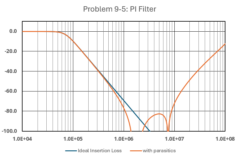
5. If this 3rd-order filter will have 20 dB of attenuation at 150 kHz, the cutoff frequency should be about 70 kHz. To make pi filter, the capacitor in parallel with the source should have an impedance of 2 Ω at 70 kHz (C1 = 1.14 μF). The capacitor in parallel with the load should have an impedance of 50 Ω at 70 kHz (C2 = 0.0455 μF). In series, their value is 0.0437 μF, so the inductor should have a value, L = 118 μH. Note that these values should probably be expressed with no more than 2 significant figures.
6. The SPICE model plots for Problems 2, 3, 4 and 5.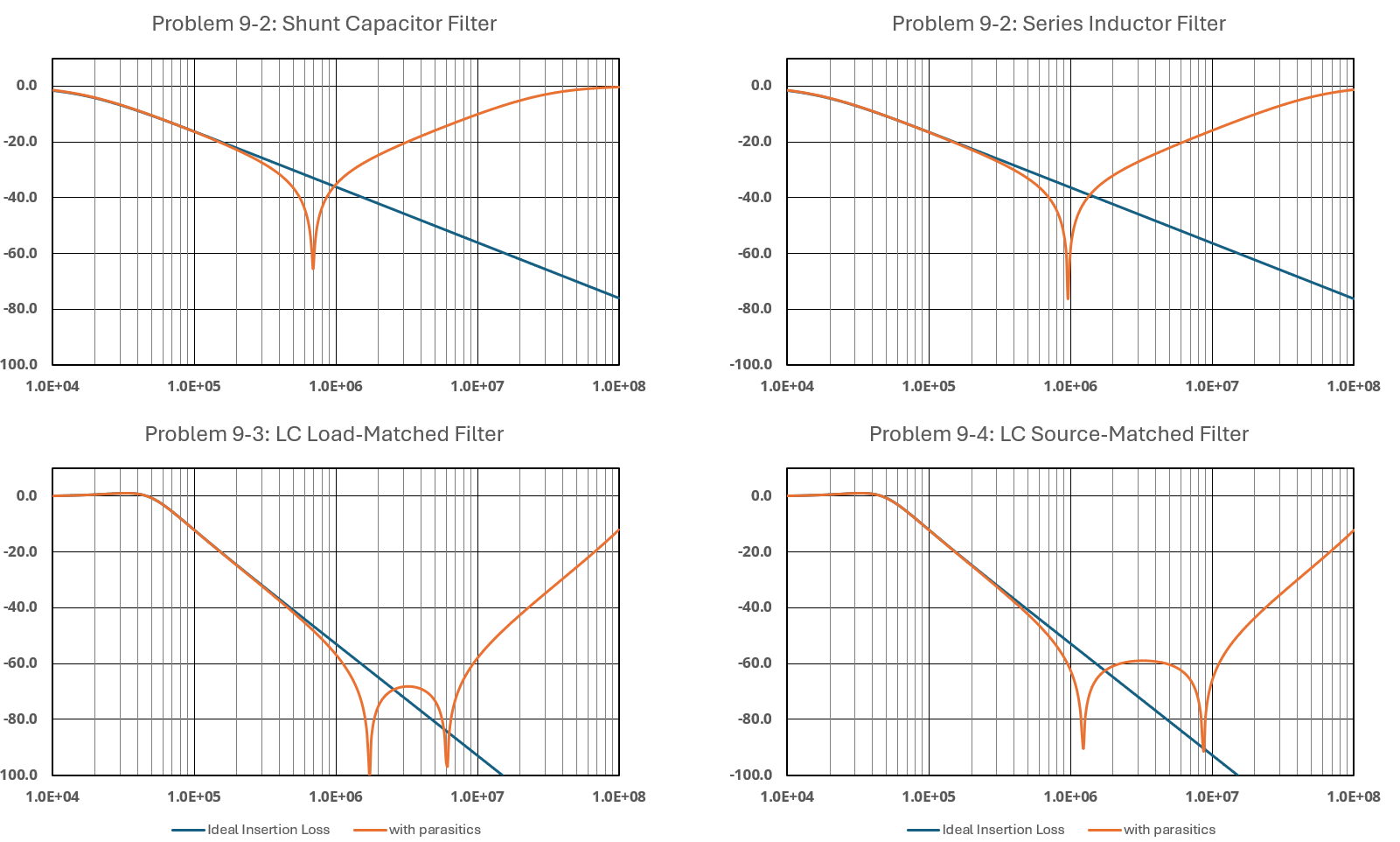
7. Option (d.) is the best layout. The input and output should never share via connections to the return plane.
8. 
9. At 10 MHz, the impedance of the source is approximately 25 - j800 Ω. Adding another 100 Ω (to get 125 - j800 Ω) doesn't significantly change the magnitude of the impedance or reduce the current. At 100 MHz, the impedance of the circuit is approximately 25 - j80 Ω. Adding another 100 Ω (to get 125 - j80 Ω) changes the magnitude of the current by a factor of 1.7 or 5 dB.
Chapters 10-12
Chapter 10 - Solutions
1. Any material with a high permeability would be appropriate. Steel would generally have the lowest cost. Mu metal would generally be the most lightweight.
2. ∇⋅B = 0. The divergence of B equal zero basically means that the total magnetic flux entering any closed volume must equal the flux leaving the closed volume.
3. (a.) Thin aluminum or copper shields are essentially invisible to a low-frequency magnetic field.
(b.) While these shields block high-frequency magnetic fields, the copper circuit board plane below them was already blocking those fields. The addition of the shield over the component generally provides little additional benefit.
(c.) These component shields are not shielded enclosures because there are usually many unfiltered traces that traverse the boundary between the inside and outside of the shielded volume.
4. Generally speaking, electrically long cable shields should only be floated at one end if connecting the shield at both ends creates a safety issue. In these situations, the shield should usually be connected to the local ground at one end and connected through a capacitor to the local ground at the other end. If no shielding is required, the shield can be floated at both ends. If only electric field shielding is required, an electrically short cable shield can be grounded at only one end.
5. Large currents can melt thin foils shields. The drain wire provides a low-resistance path for large low-frequency currents and helps to keep the bulk of this current off the foil shield. Generally, the drain wire should be connected at both ends if the foil shield is. If the foil is floated or connected through a capacitor, the drain wire is not required. In this case, if a drain wire is present, it can be connected at either end, but not both ends.
6. @1 kHz, SE = 124.4 dB, R = 136 dB, A = 0.8 dB, M =-12.2 dB.
@10 kHz, SE = 124.4 dB, R = 126 dB, A = 2.5 dB, M = -4.1 dB.
@100 MHz, SE = 341 dB, R = 86 dB, A = 255 dB, M = 0.0 dB.
@10 GHz, SE = 2618 dB, R = 66 dB, A = 2552 dB, M = 0.0 dB. [Note that values in the thousands of dB are prone to calculation errors and essentially meaningless.]
7. @1 kHz, SE = 124.4 dB, R = 59.2 dB, A = 65.2 dB.
@10 kHz, SE = 124.4 dB, R = 59.2 dB, A = 65.2 dB.
@100 MHz, SE = 341 dB, R = 296 dB, A = 45 dB.
@10 GHz, SE = 2618 dB, R = 34 dB, A = 2584 dB. [Note that values in the thousands of dB are prone to calculation errors and essentially meaningless.]
8. @10 GHz, SE = 3 dB, R = 2.25 dB, A = 0.0 dB, M = 0.75 dB.
9. @10 GHz, SE = 3 dB, R = 3 dB, A = 0.0 dB.
10. For a shielded enclosure made of any reasonable shielding material, very little energy escapes the enclosure by passing through the shielding material. The seams and apertures tend to be a much bigger factor affecting the enclosure shielding effectiveness. If the material surface doesn't have a very low resistivity, it won't make good contact when pressed against other surfaces. A leaky seam will be formed wherever two pieces of the material come together. Low surface resistivity also makes it difficult to make good connections to cable connector shields.
Chapter 11 - Solutions
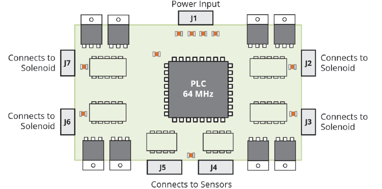 1. For the vending machine controller board shown on the right,
(a.) There is no EMC ground on this board. External connections are made on all four sides and there is no chassis ground connection.
(b.) Potential conducted emissions issues are power converter noise and any coupled high-frequency noise that drives the chassis or other cables relative to the power cable. The best option is to provide differential-mode filtering on the power input and prevent any of the PLC clock harmonics from leaving the PLC chip package.
(c.) The main potential radiated emission issue is that ANY high-frequency currents flowing on the board can drive one cable relative to another. The best option is to prevent any of the PLC clock harmonics from leaving the PLC chip package. The chip package is too small to radiate, and no high-frequency currents are required for the board to perform its intended function. All transition times can be slowed to 100 ns or longer.
(d.) ESD should be expected on the cable inputs whose routing takes them in areas where a charged person or object might make contact. Since all the interfaces are electrically slow, series resistors and TVS diodes can be placed on those interfaces if they make a direct connection to a semiconductor input.
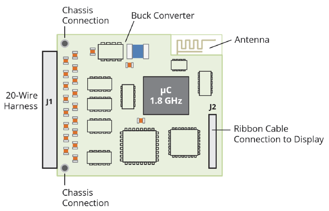 2. For the vehicle control board shown on the right,
(a.) The PCB EMC ground is the region of the return plane near the J1 connector.
(b.) The main conducted emission issues are the noise from the buck converter and any high-frequency voltage that drives the display's ribbon cable relative to the chassis ground. The buck converter is well placed, so properly minimizing the switching voltage node area and the switching current loop area and proper filtering of the differential-mode noise should eliminate the converter as a source of conducted emissions. The J2 connector is poorly placed. If it is a relatively short ribbon cable to a small display, it should be a problem at conducted emissions frequencies. Otherwise, it may be necessary to take additional steps such as shielding the circuitry between J1 and J2, or relocating J2.
(c.) The poor location of the J2 connector is also the main radiated emission issue. Shielding the circuitry or relocating J2 are possible options. Adding chassis ground connections near the J2 connector is another option.
(d.) The cables are the potential entry points for ESD currents. Evaluate each input to determine the likelihood of being exposed to ESD (during compliance testing and in the field). Provide appropriate transient protection on any input that makes a direct connection to a sensitive component.
Note: The proximity of the buck converter to the circuit board antenna is likely to be an issue. If these circuits can't be separated, it may be necessary to put a shield over the switching traces and components of the converter.
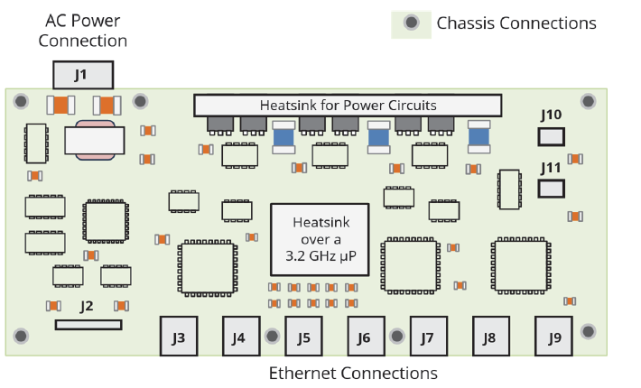 3. For the Ethernet switch circuit board shown on the right,
(a.) There are PCB grounds at the AC power connection, J1, and the front edge of the board, J2-J9. There is also a single chassis connection in the back corner near J10 and j11.
(b.) The main conducted emissions sources would be the power converter near J1 and/or the power circuits utilizing the large heatsink. Balanced DM and DM filtering on the power input at J1 is critical. The power circuit heatsink should be connected to the chassis or positioned so that field lines emanating from the heatsink are captured by the chassis.
(c.) The design relies on proper implementation of the ethernet connections (with a transformer and CM choke) to meet radiated emissions requirements. Filter the cables connected to J2, J10 and J11. In addition, the heatsink over the microprocessor could be an emissions source if it is not well connected to the board or the board is not inside a metal enclosure. Look for structures such as sparsely populated planes that might resonate at GHz frequencies.
(d.) ESD is likely to come in on the external cable connections, J2, J10 and J11 if they leave the enclosure. The Ethernet connections are probably ok. If the board is not in a metal enclosure, look for sneak paths that might allow a discharge to reach the board directly.
4. Power distribution on the vending machine board could be done with a plane on Layer 3 or using wide power traces. Either way, there should be local decoupling capacitors near each power input pin on every active device. Each decoupling capacitor should have its own via connecting directly to the ground plane on Layer 2.
3.3 V power distribution on the vehicle control board should be on a plane. This plane should be on a layer adjacent to one of the ground layers. 3.3-V decoupling capacitors should be connected directly to the planes with the lowest possible connection inductance. The location is not critical, but capacitors should be distributed around the plane. The 12-V power distribution could probably be done with a wide trace and employ local decoupling.
Power distribution on the Ethernet switch should be done on planes. All of these planes should be on the same layer (in this case, Layer 3). Decoupling capacitors should be connected directly to the planes with the lowest possible connection inductance. The location is not critical, but capacitors should be distributed around each plane. It's important to ensure that no plane has large areas with no capacitor connections, since radiated directly from the planes is possible at GHz frequencies.
5. Connection inductance is the most important parameter for a high-frequency decoupling capacitor. Class 2 ceramic capacitors pack sufficient capacitance (e.g., >0.01 μF) into the smallest package sizes. This facilitates low-inductance connections to circuit board planes. Class 1 ceramic capacitors tend to be larger and more expensive for a given nominal value of capacitance. Note that Class 2 ceramic capacitors should not be used to decouple AC power inputs. Their non-linear behavior with varying voltages can generate harmonics of the AC power frequency.
6. 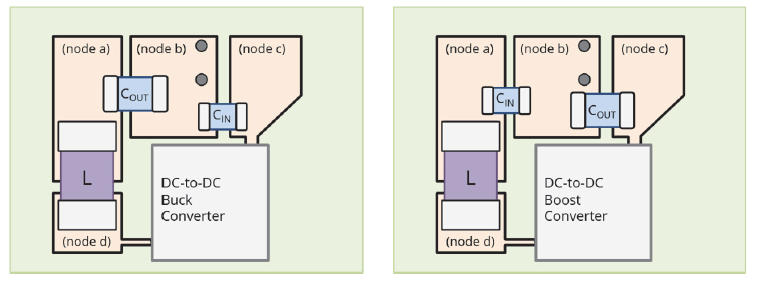 For the buck converter, the switching voltage is on node (d). The switching current flows from the converter IC, through CIN to the ground plane, then back to the converter. In this layout, node (b) should be eliminated and both CIN and COUT should connect directly to the ground plane.
For the boost converter, the switching voltage is also on node (d). The switching current flows from the converter IC, through COUT to the ground plane, then back to the converter. In this layout, node (b) should be eliminated and both CIN and COUT should connect directly to the ground plane. Note the similarity between the optimum buck and boost converter layouts when VIN and VOUT are exchanged.
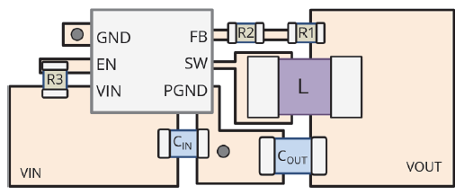 7. The switching voltage node is the trace connecting the SW pin to the inductor. The switching current loop is from the VIN pin to CIN to PGND to GND plane and back to the IC. This is a poor layout. No converter switching a 100 kHz or faster should have an isolated PGND. CIN and COUT should connect directly to the GND plane. The switch node should be so close to R2.
8. Power dissipated as heat in a linear regulator:
(a.) Regulator must drop 0.5 volts while supplying 60 A of current. Power dissipated = 30 W.
(b.) Regulator must drop 0.5 volts while supplying 6 mA of current. Power dissipated = 3 mW.
(c.) Regulator must drop 8.7 volts while supplying 6 mA of current. Power dissipated = 52 mW.
(d.) Regulator must drop 8.7 volts while supplying 6 A of current. Power dissipated = 52 W.
9. The efficiency of a power converter is the ratio of the power out to the power in.
(a.) Power output = 11.5 V x 60 A = 690 W, therefore at 95% efficiency the power input is 726 W. Power dissipated = 36 W.
(b.) Power output = 11.5 V x 6 mA = 69 mW, therefore at 95% efficiency the power input is 72.6 mW. Power dissipated = 3.6 mW.
(c.) Power output = 8.7 V x 6 mA = 52 mW, therefore at 95% efficiency the power input is 55 mW. Power dissipated = 3 mW.
(b.) Power output = 8.7 V x 6 A = 69 W, therefore at 95% efficiency the power input is 72.6 W. Power dissipated = 3.6 W.
Note that the buck converter is much more efficient in cases (c.) and (d.) where the voltage drop is significant. The linear regulator is often a good choice when the voltage drop is a small fraction of the original voltage.
10.
Quiz Question: Are capacitors with a small nominal value better than capacitors with a high nominal value for high-frequency decoupling?
Answer is NO.
Publications that advocate this tend to make the incorrect assumption that capacitors don't provide decoupling at frequencies above the self-resonant frequency of the capacitor.
Quiz Question: Some design guidelines state that capacitors must be located within a radius of the active device equal to the distance a wave can travel in the transition time of the circuitry. Is this correct?
Answer is NO.
Publications that advocate this fail to differentiate between the low characteristic impedance of closely spaced planes and the high characteristic impedance (or inductance) of the connections to surface-mounted decoupling capacitors. They ignore the frequency range where surface mount capacitors are effective when there are closely spaced power planes. They also ignore the time-harmonic nature of power bus noise sources and plane resonances.
Quiz Question: Some design guidelines state that it is advantageous to alternate the polarity of decoupling capacitor connections so that one capacitor's VCC
connection is close to another capacitor's GND connection. Is this correct?
Answer is usually NO.
Publications that advocate this assume the inductance of the loop formed by the vias between the top of the board and the planes dominates the overall connection inductance. This can only happen when the vias travel a significant distance (e.g. 8 layers) into the board before reaching the plane pair. While this scenario is possible, it is not likely in situations where it's important to minimize the power distribution impedance.
Chapter 12 - Solutions
1. (a.) Mu-metal shields are relatively expensive, so they are not likely to be used in high-volume products where cost is a high priority. Steel is usually a good alternative, but steel shields are relatively heavy. One application where weight is often a higher priority than cost is aerospace designs. Of the industries listed in Table 12.1, it is the one most likely to utilize mu-metal shields.
(b.) Embedded capacitance is also relatively expensive, but it is excellent at reducing high-frequency power bus noise. It is most likely to be used in very fast circuit boards in industries where weight or complexity is a higher priority than cost. This would include some military and aerospace applications.
(c.) Isolated power converters are required in applications where at least one of the working voltages is greater than about 50 volts. This includes all products that are powered from an AC wall outlet, so examples of isolated power converters are found in all of the industries listed in Table 12.1. Medical and aerospace products often have additional requirements that prohibit power currents from flowing on the ground structure, so isolated converters are even more prevalent in those industries.
(d.) Latch-up resistant CMOS is used in many safety critical applications where exposure to electrical transients is expected. This technology can be found in some military, aerospace and automotive applications.
(e.) Filter-pin connectors can be very effective, but they are generally more expensive than filter done on a printed circuit board. They are most likely to be found in military and aerospace products that utilize fully shielded enclosures. When they are found on products in other industries, it is often because a last-minute fix was needed to bring a product into compliance.
2. Making a high-speed digital interface immune to interference from ESD without employing error detection and correction is not trivial. Typically, the signal path must be well shielded at every point between the source and the receiver. This can be a prohibitively expensive requirement in consumer electronics or industrial controls. On the other hand, it can often be justified in safety critical communications where milliseconds or even microseconds of delay might be a problem. Generally, it's important to recognize that some EMC requirements can have a significant cost associated with them. Borrowing the requirements from one product's EMC test plan to write the test plan for another product can have serious implications affecting cost and development time.
3. Possible errors or omissions that cause a conducted emissions problem:
- inadequate powerline filter design (e.g. wrong component values or incorrect electrical balance)
- poor powerline filter layout (e.g. parasitics allow noise to bypass the filter)
- poor power converter layout (e.g. coupling from switch node or switching current loop that carries noise away from converter)
- poor grounding strategy (e.g. no PCB EMC ground or filtering to the wrong ground)
- replacement of one or more existing powerline filter components
- addition of a ferrite core on the cable (for HF CM problems)
- filter-pin power connector
4. Possible reasons for differences between radiated emissions measurements in different labs.
- different cable layouts
- different cable terminations
- different supporting equipment connected to DUT
- different test personnel, equipment settings, antenna types
- size and shape of tabletop
- size and shape of the room
- method of grounding the tabletop to the floor or wall
- antenna calibration factor (because antenna is not in the far field)
5. Possible errors or omissions that cause a radiated emissions problem (< a few hundred MHz):
- poor grounding strategy (e.g. no PCB EMC ground or filtering to the wrong ground)
- high-frequency content on an I/O line that is unshielded or improperly filtered
- poor cable shield termination (e.g. high impedance or terminated to wrong location)
- high-frequency electric fields from components or heatsinks not properly captured by board or enclosure
Possible fixes that don't involve a new board layout (< a few hundred MHz):
- replacement of one or more existing I/O filter components
- addition of a ferrite core on the cable
- changes to connector design (e.g. filter-pin connectors, cable shield connections)
- changes to enclosure design (e.g. for better shielding)
- relocate cables or floating conductors near a circuit board that might be carrying noise current
- Parasitic oscillations (e.g. between ceramic capacitors with very different nominal values)
- cavity resonances between circuit board planes
- enclosure cavity resonances driving seams or apertures
Possible fixes that don't involve a new board layout (GHz):
- remove or replace components involved in a parasitic oscillation
- seal up seams using gaskets or additional fasteners
- make a small change to the operating frequency of a component driving a cavity resonance
- use lossy materials to dampen cavity resonances
6. Automotive and aerospace systems tend to have many systems packed into a relatively small volume. Some are big noise producers, and some are very sensitive to noise. In addition, these systems tend to operate in a wide variety of electromagnetic environments while performing safety-critical functions. The wiring harnesses in automotive and aerospace equipment represent the main coupling path for bringing noise into the various system components. The best way to evaluate a product's immunity to noise on the wiring harness is to inject noise directly onto the harness. Most consumer devices do not have a wiring harness. If they have attached cables, these cables unlikely to be bundled or routed near to strong RF sources. In most cases, the coupling to any attached cables in consumer devices is addressed by radiated immunity tests. Computing equipment in a data center may have wiring harnesses, but data center electromagnetic environments are relatively controlled. Often, in these environments, radiated immunity testing is done on location using equipment that generates strong fields rather than injecting currents directly onto a harness.
7. Possible errors or omissions that cause an electrostatic discharge problem:
- missing or inadequate transient protection (e.g. component too slow or no impedance between transient protection and IC input)
- ESD can reach unprotected components or circuits
- inadequate filtering of low-speed IC digital inputs that allows them to respond to fast transients
- poor grounding strategy (e.g. no PCB EMC ground or filtering to the wrong ground)
Possible fixes that don't involve a new board layout:
- replace components with "ESD rated" components (e.g. when filter capacitors or resistors are damaged by ESD)
- add a potting material or cover designed to prevent discharges directly to the board
- change the enclosure design or materials to dissipate charge
- warning label or ESD handling guidelines
8. Radiated emissions and ESD immunity. A 1-kΩ resistor in series with the pins of an IC can essentially block high-frequency clock harmonics that are often coupled out of the IC on these pins. This is an important tool that can help to guarantee compliance with radiated emissions requirements. A 1-kΩ resistor in series with the low-speed digital input pins of an IC can prevent that input from unintentionally responding to indirect coupling from ESD transients.
9. In this example, the reliable operation of a safety-critical system depends on a single capacitor. Capacitors frequently fail with time or when exposed to transients. Since the failure of a filter capacitor would typically be undetectable, this system is still vulnerable. Other mitigating design features are still required. These features should not rely on the proper operation of any one component or system. However the problem is solved, the product design must document the problem and the solution, and it must be part of the Failure Mode Effects Analysis (FMEA) performed for the vehicle.
10. (a.) Design Rule: Always minimize the loop area of high-speed circuits. This is never really necessary unless the circuit is the source of unwanted coupling or radiated emissions. For example, when a circuit board traced needs to be routed between Point A and Point B, the shortest, most direct route may be a path that creates crosstalk or signal integrity issues. In that case, it is better to route the trace away from sensitive circuits or discontinuities even if that path length is much longer.
(b.) Design Rule: Locate decoupling capacitors near the power pins they are decoupling. As discussed in Chapter 11, on boards with closely spaced power planes the location of the high-frequency decoupling capacitors is not critical. If locating a decoupling capacitor near each of the power pins creates routing issues or crosstalk problems in a board with closely spaced power planes, then this design rule creates more problems than it solves.
(c.) Design Rule: Locate high-speed devices far from the I/O connectors. This design rule from the 1980s was only appropriate for certain specific systems at the time. High-speed circuits associated with digital interfaces should generally be located very close to their respective I/O connectors. Locating a high-speed transceiver far from its I/O connector would mean routing high-speed traces a greater distance across the board. This make routing more difficult and provides more opportunities for unwanted coupling.
(d.) Design Rule: Digital signal transition times should be 0.1 times the bit width or slower. This is a good idea in general but is not always necessary or desirable. If the signal path is relatively short, or it is clear that no significant signal power can be coupled to other circuits, then slowing the transition time is unnecessary. Also, for very slow bit rates (e.g., 500 kbps or less), the bit width is very long. If a transition time is slowed too much (e.g. >200 ns), the signal spends too much time at an amplitude halfway between the low and high states. At this amplitude, relatively small levels of noise on the input can cause unwanted switching of the output.