
Bad EMC Advice Recently Spotted on the Internet
The internet is a convenient way to find information on EMC and signal integrity. Unfortunately, much (perhaps most) of the information related to EMC design is either not helpful or just plain wrong. Here are recent sightings of bad EMC design advice from a variety of internet sources.
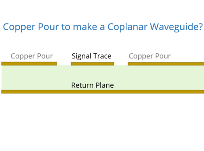
Claim: Circuit boards with RF traces should have a ground pour on the top layer.
Sighted: PCB Supplier on social media site (June 6, 2026)
Why this is bad advice: Ground pour on the outer layers of a multi-layer circuit board is generally not recommended unless it is for heat dissipation and/or copper balancing. Microstrip RF traces routed 0.25 mm or less above a return plane have a relatively stable impedance and do not generally benefit from a copper pour. In fact, any copper pour that comes too close to the RF trace can introduce EMC and signal integrity problems.
more ...
Reasons often cited for using a ground pour include:
- Ability to achieve a lower characteristic impedance with a thinner trace. But no space is saved, because maintaining a uniform ground pour on both sides of a trace requires even more space than a wide trace.
- Reduced crosstalk to nearby traces. But copper pours are not a particularly effective or reliable way to reduce crosstalk when the return plane is 0.25 mm or less below the signal traces. Proper lateral spacing of the signal traces achieves the same isolation with no danger of introducing unwanted resonances or coupling signal power to nearby structures through the plane structure.
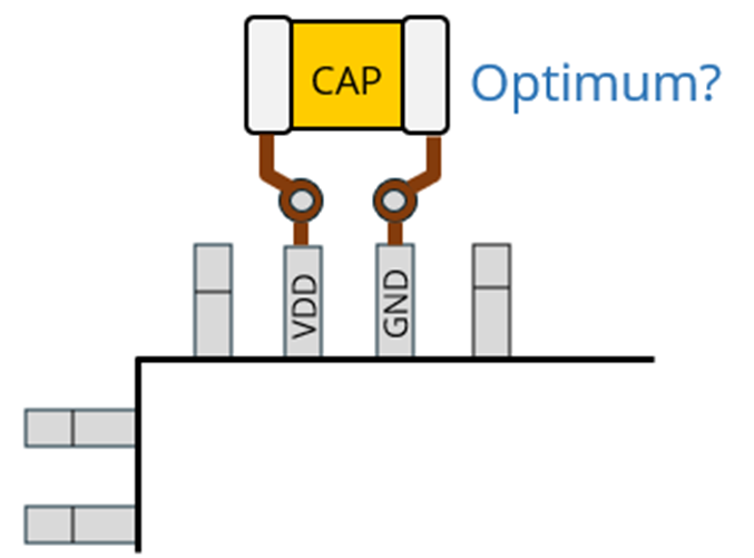
Claim: Local decoupling capacitors should share power and ground vias with the devices they are decoupling.
Sighted:
PCB Supplier website (July 9, 2026)
PCB design consultant on social media site (June 7, 2026)
Why this is bad advice: The rules for optimum decoupling capacitor placement and selection depend on many factors, including the plane spacing, component packaging, and target impedance. There is no rule for optimum placement that is going to work in all cases. Beyond that, the rule cited above is NEVER optimum. There is no situation where sharing power and ground vias provides the lowest-inductance connection or the lowest possible power bus noise.
more ...
Even if the spacing between power and ground pins of the active device happens to match the length of the decoupling capacitor (as often depicted in drawings accompanying this advice), sharing a via connection to the ground plane unnecessarily increases the inductance of ground connection for one or both components. A good rule of thumb for any component operating at high frequencies is that every connection to the ground plane should be done at the component pin (i.e., no ground traces). This minimizes ground bounce in active devices and minimizes the connection inductance of decoupling capacitors.
In most cases, the spacing between active device power and ground pins is not a good match for the decoupling capacitor length. In those situations, trying to share power and ground via connections forces the designer to use traces to make one or both connections. This adds inductance and potentially interferes with the routing of other signal traces.
Of course, most devices in SOIC, QFP or TSOP packages don't have really low target impedances. For these devices, the capacitor mounting indicated in the drawing is probably fine. However, it is never optimum and certainly not convenient. If high-frequency decoupling is important, then don't rely on guidelines like this. Take the time to get it right for your particular application.
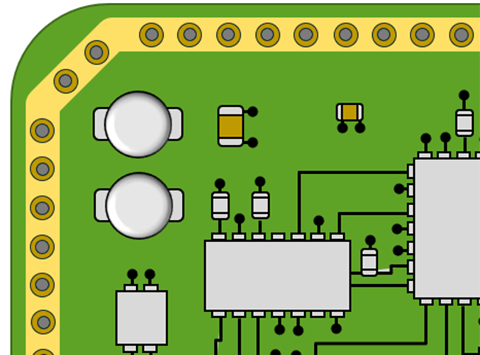
Claim: A ground trace along the perimeter of the board on all layers will reduce emissions from the edges.
Sighted:
PCB Supplier website (July 9, 2026)
PCB Supplier on social media site (June 22, 2026)
Why this is bad advice: There are certain applications where placing a ground trace at specific locations around the board perimeter makes sense. Those applications generally involve making a good connection to a metal enclosure or perhaps for ESD protection in devices with a plastic enclosure. They never involve creating a Faraday cage or reducing radiation from the edge of the board.
more ...
Faraday cages only work if no conductors penetrate the boundary. Stitching the edges of the ground planes in a circuit board doesn't prevent power from coupling into and out from the traces and vias between the planes. In some situations, stitching around the perimeter of a resonant cavity can actually enhance this coupling.
Of course, one could argue that radiation from the edges of the cavity formed by the planes is reduced. But the most effective way to reduce edge radiation from a cavity is to stitch the planes together at many points randomly throughout the cavity. This prevents the cavity from resonating and eliminates any significant edge radiation. It is not necessary or desirable to make the majority of these connections around the board's perimeter.
Another important point is that a ground trace around the board's perimeter on the outer layers does not prevent or reduce radiated emissions from the board. Yes, it can change the field patterns near the edge and, sometimes, this is desirable. On average though, it doesn't reduce the field strength. It just changes the location. Ground traces around the board perimeter should never be the default. They should only be used in specific situations to meet a well-defined goal.
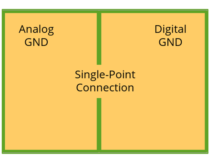
Claim: Analog grounds should be isolated from digital grounds.
Sighted:
PCB Supplier on social media site (June 22, 2026)
Why this is bad advice: First, let's not confuse the concept of ground with the concept of current-return. Reference grounds are never isolated for EMC or signal integrity reasons. On the other hand, low-frequency current-returns are sometimes isolated to prevent common-impedance coupling. Back in the days when most boards had 1 or 2 layers, and signal frequencies were typically measured in kilohertz, isolating digital signal returns from analog signal returns was an important part of meeting EMC and signal integrity requirements. But those days are long gone. Today, isolating analog and digital returns is rarely necessary or desirable. In rare situations where a low-frequency analog return needs to be isolated from the digital return plane in a circuit board, the returns should be routed on different layers. Only one of the returns should be a plane; the other should be routed on traces.
more ...
Since planes and traces labeled "ground" are often the reference voltage for signals leaving the circuit board, it is often necessary to bond them at high frequencies even if they are isolated at low frequencies. This adds cost and takes up space, so current-returns should only be isolated when it is absolutely necessary. The test to determine when isolation is necessary is easy to perform. Multiply the worst-case DC resistance of the shared return path by the maximum low-frequency current in the source circuit. If the resulting voltage would disrupt the operation of the victim circuit, and filtering won't help, then isolation is required.
Note that there are often legitimate safety-related reasons for isolating high-voltage current-returns from system ground. For more information see our tutorial on Grounding.
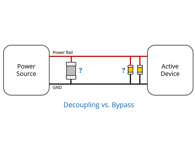
Claim: Decoupling capacitors and bypass capacitors serve different purposes.
Sighted:
Multiple PCB supplier websites (July 10, 2026)
PCB Supplier on social media site (June 24, 2026)
Why this is bad advice: There is no widely accepted definition of a decoupling capacitor as opposed to a bypass capacitor. Both are connected across DC power rails. Both are used to stabilize the power bus voltage. AI-generated memes often claim that one of them provides local decoupling while the other provides global decoupling, or that one filters noise from the power supply while the other filters noise from the circuits. In reality, these terms are not defined that way, and the advice offered by sites that make this distinction is almost always wrong.
more ...
The local vs. global decoupling capacitor distinction is important, but a capacitor that provides local decoupling on one board might be used to provide global decoupling on another board. There are no specific properties of the capacitor itself that determine whether it is local or global.
The term "bulk capacitor" is often used to describe capacitors with a relatively large nominal value that are designed to provide global low-frequency decoupling. High-frequency decoupling is generally provided by ceramic capacitors in small packages. These can be local or global depending on the powerbus geometry and the decoupling strategy employed. For more information, see our article titled Circuit Board Decoupling.
We welcome comments and questions. If you see something on social media that you'd like for us to include here, please let us know by sending an email to